| CPC H10D 84/834 (2025.01) [H10D 30/024 (2025.01); H10D 30/6211 (2025.01); H10D 30/6219 (2025.01); H10D 64/01 (2025.01); H10D 64/512 (2025.01); H10D 84/05 (2025.01); H10D 30/6735 (2025.01)] | 12 Claims |
|
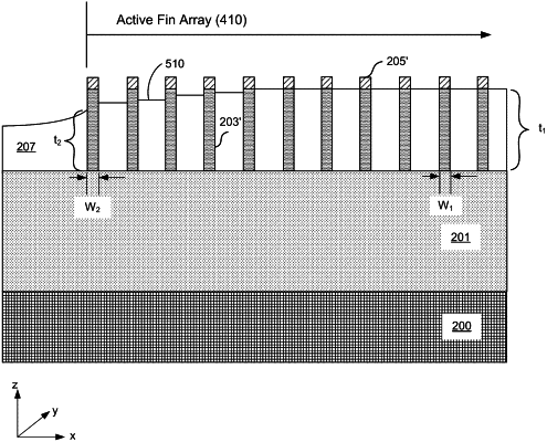
1. A vertical, fin-based field effect transistor (FinFET) device comprising:
an array of individual FinFET cells, the array comprising a plurality of rows and columns of separated fins, wherein each of the separated fins is in electrical communication with a source contact;
one or more rows of first inactive fins disposed on a first set of sides of the array of individual FinFET cells;
one or more columns of second inactive fins disposed on a second set of sides of the array of individual FinFET cells; and
a gate region surrounding the individual FinFET cells of the array of individual FinFET cells, the first inactive fins, and the second inactive fins.
|