| CPC H10D 62/107 (2025.01) [H01L 21/046 (2013.01); H10D 62/8325 (2025.01)] | 20 Claims |
|
1. A method of manufacturing a semiconductor structure, comprising:
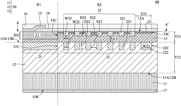
forming a substrate of the semiconductor structure, the substrate comprising a first silicon carbide layer and a second silicon carbide layer under the first silicon carbide layer, and the substrate comprising a unit region and a termination region surrounding the unit region;
forming a first guard ring structure in the termination region and in the first silicon carbide layer, the first guard ring structure adjoining a top surface of the first silicon carbide layer, and including a plurality of first guard ring well regions; and
forming a second guard ring structure in the termination region and in the second silicon carbide layer, the second guard ring structure including a plurality of second guard ring well regions; and
wherein the plurality of second guard ring well regions correspond one-on-one to the plurality of first guard ring well regions, and each of the plurality of second guard ring well regions overlaps with a corresponding one of the plurality of first guard ring well regions in a vertical direction.
|