| CPC H10B 53/30 (2023.02) [H01L 23/5226 (2013.01); H10B 69/00 (2023.02)] | 20 Claims |
|
1. A device, comprising:
a first region comprising:
a first conductive interconnect within a first dielectric in a first level, the first conductive interconnect comprising a first lateral thickness; and
a second level above the first level, the second level comprising:
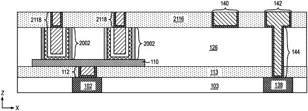
an electrode structure on the first conductive interconnect, the electrode structure comprising a first conductive hydrogen barrier layer and a first conductive fill material, wherein the electrode structure comprises a second lateral thickness;
an etch stop layer laterally surrounding the electrode structure;
a plate electrode on the electrode structure, the plate electrode extending beyond a perimeter of the electrode structure and on the etch stop layer;
a second dielectric on the plate electrode and on the etch stop layer;
a plurality of trenches within the second dielectric;
a plurality of trench capacitors on the plate electrode, wherein individual ones of the plurality of trench capacitors is in individual ones of the plurality of trenches, and wherein the individual ones of the plurality of trench capacitors comprise:
a dielectric spacer along a sidewall of the individual ones of the plurality of trenches;
a first electrode on a base and on the dielectric spacer along the sidewall of the individual ones of the plurality of trenches, wherein the first electrode is in contact with the plate electrode;
a dielectric layer comprising a ferroelectric material or a paraelectric material substantially conformal to the first electrode; and
a second electrode in contact with the dielectric layer; and
a plurality of via electrodes wherein, individual ones of the plurality of via electrodes is on the second electrode of the individual ones of the plurality of trench capacitors, wherein the individual ones of the plurality of via electrodes comprise:
a second conductive hydrogen barrier layer comprising a lateral portion in contact with the second electrode and substantially vertical portions connected to the lateral portion; and
a second conductive fill material adjacent to the second conductive hydrogen barrier layer; and
a second region adjacent to the first region, the second region comprising:
a second conductive interconnect within the first dielectric in the first level and wherein the second level further comprises:
a metal structure; and
a via structure coupled between the second conductive interconnect and the metal structure, wherein at least a first portion of the via structure is adjacent to the etch stop layer, and a second portion of the via structure is adjacent to the second dielectric.
|