| CPC H03D 3/007 (2013.01) [H04L 27/227 (2013.01); H04L 27/2273 (2013.01); H04L 27/233 (2013.01); H04L 27/3872 (2013.01); H04L 2027/0057 (2013.01)] | 18 Claims |
|
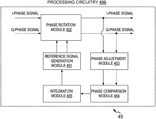
1. A demodulation device comprising:
processing circuitry configured:
to rotate phases of an I-Phase signal and a Q-Phase signal in a received signal of a multilevel PSK signal using a reference signal;
to adjust the phases of the phase rotated I-Phase signal and the phase rotated Q-Phase signal by multiplying the phases of the phase rotated I-Phase signal and the phase rotated Q-Phase signal with an integer value to generate a phase adjusted I-Phase signal and a phase adjusted Q-Phase signal;
to compare the phase of the phase adjusted I-Phase signal with the phase of the phase adjusted Q-Phase signal to generate a phase comparison result; and
to generate a reference signal using the phase comparison result.
|