| CPC H02M 7/53871 (2013.01) [H02M 1/0006 (2021.05); H02M 1/32 (2013.01); H02M 7/05 (2021.05); H02M 7/2173 (2013.01); H03K 17/08104 (2013.01); G05F 1/571 (2013.01); H02M 5/453 (2013.01); H02M 5/458 (2013.01)] | 20 Claims |
|
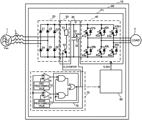
1. A power conversion device comprising:
a converter circuit (20) configured to convert AC electric power output from an AC power source (1) into DC power;
an inverter circuit (40) including a plurality of switching elements (41a to 46a), and configured to convert the DC power into AC power to supply the AC power to a load;
a capacitor (31) connected in parallel to each of the converter circuit (20) and the inverter circuit (40) between the converter circuit (20) and the inverter circuit (40), the capacitor (31) allowing variation of an output voltage from the converter circuit (20), the capacitor (31) absorbing variation of an output voltage from the inverter circuit (40) due to a switching operation; and
a control circuit (60, 70) configured to control the inverter circuit (40), wherein
when supply of power from the inverter circuit (40) to the load is stopped, the control circuit (60, 70) performs turn-on control to turn at least one of the switching elements (41a to 46a) on so that an absolute value of an average output power from the inverter circuit (40) is less than if all of the switching elements (41a to 46a) are turned off, and
the turn-on control is performed to switch the output power from the inverter circuit (40) between positive and negative values during a switching period for the switching elements (41a to 46a) so that the average output power from the inverter circuit (40) during the switching period is substantially zero.
|