| CPC H02M 7/003 (2013.01) [H02M 7/48 (2013.01); H05K 7/02 (2013.01); H05K 7/20 (2013.01); H05K 9/0081 (2013.01)] | 17 Claims |
|
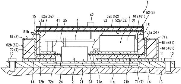
1. A power converter comprising:
semiconductor modules;
a capacitor electrically connected to the semiconductor modules;
a circuit board;
a casing accommodating the circuit board, the semiconductor modules and the capacitor;
a busbar having an input terminal portion, an output terminal portion and an electric pathway connecting the input terminal portion and the output terminal portion, the electric pathway being connected to at least one of electronic components including the semiconductor modules and the capacitor, the busbar having a built-in portion incorporated into the casing;
a shield layer electrically conductive and provided on an inner surface or an outer surface of the casing such that the shield layer covers the built-in portion;
a cooling member configured to cool the semiconductor modules; and
a cooling side seal electrically conductive and interposed between the casing and the cooling member for sealing a gap between the casing and the cooling member, wherein
the shield layer includes an outer layer provided on the outer surface of the casing such that the outer layer covers the built-in portion, and
the cooling side seal is in contact with the outer layer.
|