US 12,261,350 B2
Semiconductor device package and method of manufacturing the same
Guo-Cheng Liao, Kaohsiung (TW); and Yi Chuan Ding, Kaohsiung (TW)
Assigned to ADVANCED SEMICONDUCTOR ENGINEERING, INC., Kaohsiung (TW)
Filed by Advanced Semiconductor Engineering, Inc., Kaohsiung (TW)
Filed on Aug. 8, 2023, as Appl. No. 18/231,771.
Application 18/231,771 is a continuation of application No. 17/222,875, filed on Apr. 5, 2021, granted, now 11,721,884.
Application 17/222,875 is a continuation of application No. 16/375,640, filed on Apr. 4, 2019, granted, now 10,971,798, issued on Apr. 6, 2019.
Claims priority of provisional application 62/747,580, filed on Oct. 18, 2018.
Prior Publication US 2023/0402738 A1, Dec. 14, 2023
Int. Cl. H01Q 1/38 (2006.01); H01L 21/48 (2006.01); H01L 23/498 (2006.01); H01L 23/66 (2006.01); H01Q 1/22 (2006.01)
CPC H01Q 1/2283 (2013.01) [H01L 21/48 (2013.01); H01L 21/4853 (2013.01); H01L 23/498 (2013.01); H01L 23/49816 (2013.01); H01L 23/66 (2013.01); H01Q 1/22 (2013.01); H01Q 1/38 (2013.01); H01L 2223/6677 (2013.01)] 20 Claims
OG exemplary drawing
 
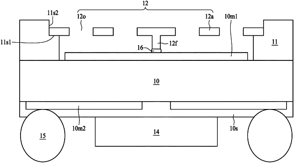
1. A semiconductor device package, comprising:
a first antenna comprising an antenna pattern, wherein the antenna pattern has a first portion and a second portion spaced apart from the first portion; and
a second antenna disposed over the first antenna and having an opening exposing the second portion of the first antenna pattern of the first antenna, wherein the second antenna comprises a conductive material.