| CPC H01L 27/0629 (2013.01) [H01L 27/0605 (2013.01); H01L 28/60 (2013.01); H01L 29/2003 (2013.01); H01L 29/402 (2013.01); H01L 29/7786 (2013.01)] | 9 Claims |
|
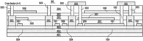
1. An integrated circuit, comprising:
a gallium nitride field effect transistor (GaN FET) including gate metal formed of a gate metal layer;
a GaN layer above a substrate; and
a front barrier layer above the GaN layer;
wherein a two-dimensional electron gas (2DEG) is formed at the interface between the GaN layer and the front barrier layer;
a first field plate disposed over the GaN FET and formed of a field plate metal layer;
a capacitor including:
a bottom electrode formed of the gate metal layer, wherein the bottom electrode of the capacitor is electrically connected to the 2DEG by an Ohmic contact; and
a top electrode formed of the field plate metal layer, wherein the bottom electrode of the capacitor has a portion formed in the shape of a ring surrounding the conductive via, wherein the ring forms a diode with respect to a portion of the 2DEG underlying the ring, to block current flow and increase the voltage breakdown capability of the capacitor in a first polarity direction, when the top electrode is at a higher voltage than the bottom electrode;
a contact to the top electrode comprising a conductive via which extends through the top electrode; and
a first dielectric layer disposed between the gate metal and the first field plate, and between the top electrode and the bottom electrode of the capacitor.
|