| CPC H01L 24/19 (2013.01) [H01L 21/561 (2013.01); H01L 21/568 (2013.01); H01L 24/11 (2013.01); H01L 24/96 (2013.01); H01L 25/0652 (2013.01); H01L 2224/11001 (2013.01)] | 19 Claims |

|
1. A semiconductor device, comprising:
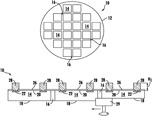
an embedded device comprising a first surface, a second surface opposite the first surface, and conductive studs disposed over the first surface;
an encapsulant disposed over at least five sides of the embedded device and around a periphery of the embedded device; and
a plurality of conductive posts disposed around the periphery of the embedded device, wherein:
sides of the plurality of conductive posts directly contact the encapsulant,
each of the plurality of conductive posts extends completely through the encapsulant and each of the plurality of conductive posts further comprises a first end and a second end opposite the first end,
the first end is exposed from the encapsulant and is coplanar with a first surface of the encapsulant and the conductive studs,
the second end is exposed from a second surface of the encapsulant opposite the first surface of the encapsulant, wherein the second end extends outwardly from a recessed portion of the second surface of the encapsulant by an offset, wherein the offset comprises a distance in a range of 5-50 μm, and each of the plurality of conductive posts are formed from a continuous, unitary material between the first end and the second end.
|