| CPC H01L 21/76275 (2013.01) [H01L 21/76254 (2013.01)] | 19 Claims |
|
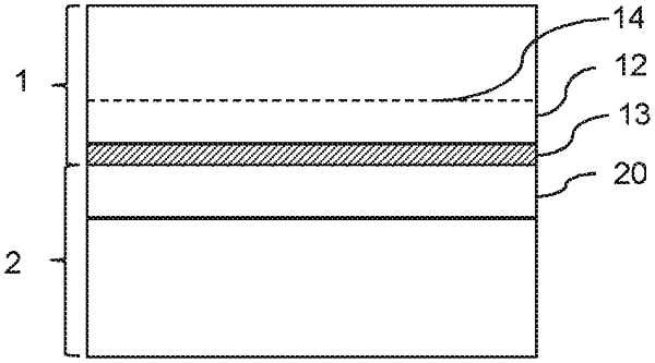
1. A strained semiconductor-on-insulator substrate, the substrate comprising:
a base substrate;
a partially relaxed monocrystalline semiconductor material disposed on the base substrate;
a dielectric layer disposed on the partially relaxed monocrystalline semiconductor material;
a partially strained monocrystalline semiconductor layer disposed on the dielectric layer;
a bonding interface buried within the dielectric layer or located between the dielectric layer and the partially strained monocrystalline semiconductor layer; and
trenches extending from a surface of the partially strained monocrystalline semiconductor layer through the partially strained monocrystalline semiconductor layer, through the dielectric layer, through the partially relaxed monocrystalline semiconductor material, and only partially into the base substrate.
|