| CPC H01L 21/268 (2013.01) [H01L 21/7813 (2013.01); H01L 21/326 (2013.01)] | 3 Claims |
|
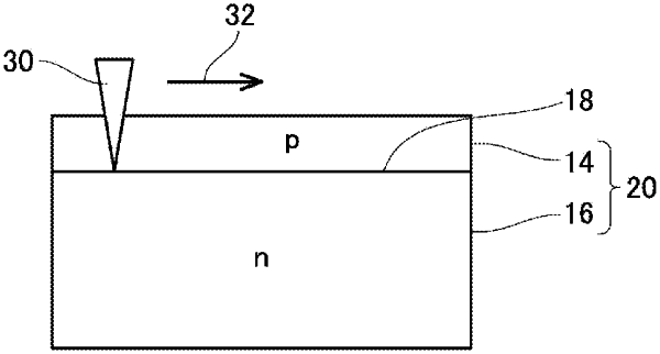
1. A method for manufacturing a semiconductor device, comprising
irradiating, with laser light, a semiconductor substrate having a p-type first semiconductor layer and an n-type second semiconductor layer so that the laser light converges on an interface between the first semiconductor layer and the second semiconductor layer, wherein each of the p-type first semiconductor layer and the n-type second semiconductor layer placed on the first semiconductor layer is formed of a compound semiconductor; and
separating the semiconductor substrate into the first semiconductor layer and the second semiconductor layer along the interface.
|