| CPC H01L 21/0332 (2013.01) [H01J 37/32899 (2013.01); H01J 37/32926 (2013.01); H01L 21/31116 (2013.01); H01L 21/31144 (2013.01); H01J 2237/334 (2013.01)] | 21 Claims |
|
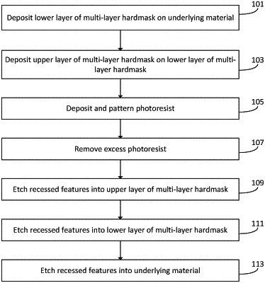
1. A method of processing a substrate, the method comprising:
a. receiving a substrate comprising:
i. underlying material,
ii. an organic planarizing layer positioned over the underlying material,
iii. a multi-layer hardmask positioned over the organic planarizing layer, the multi-layer hardmask comprising:
1. A lower layer comprising an inorganic dielectric silicon-containing material, and
2. An upper layer comprising a metal oxide, a metal nitride, or a metal oxynitride, and
iv. a layer of extreme ultraviolet (EUV) photoresist positioned over the multi-layer hardmask, wherein the layer of EUV photoresist is patterned to include recessed features, and wherein portions of the upper layer of the multi-layer hardmask are exposed within the recessed features;
b. etching the exposed portions of the upper layer of the multi-layer hardmask, thereby extending the recessed features into the upper layer of the multi-layer hardmask and exposing portions of the lower layer of the multi-layer hardmask;
c. etching the exposed portions of the lower layer of the multi-layer hardmask, thereby extending the recessed features into the lower layer of the multi-layer hardmask and exposing portions of the organic planarizing layer;
d. etching the exposed portions of the organic planarizing layer, thereby extending the recessed features into the organic planarizing layer and exposing portions of the underlying material; and
e. etching the exposed portions of the underlying material, thereby extending the recessed features into the underlying material.
|