| CPC G11C 13/0069 (2013.01) [G11C 13/0023 (2013.01); G11C 13/0064 (2013.01); G11C 2013/0066 (2013.01)] | 10 Claims |
|
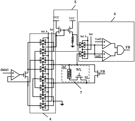
1. A memory circuit structure, comprising:
a storage array, wherein the storage array comprises at least two storage units;
a decoder connected with a bit line and a word line of the storage array, and configured to select a specific storage unit in a specific row and a specific column for operation;
a programming circuit configured to generate a voltage pulse or a constant current pulse;
a polarity switching circuit connected with the programming circuit, and configured to implement a switching between a voltage programming and a current programming of the programming circuit under a set operation and a reset operation;
a detection circuit connected with the storage array, and configured to detect a detection signal of a current or a voltage corresponding to the specific storage unit in the storage array and feed back the detection signal to a control unit, wherein the detection signal output by the detection circuit is configured to enable the polarity switching circuit to switch; and
the control unit configured to, according to the detection signal, control the polarity switching circuit to perform a switching operation and control a pulse output of the programming circuit.
|