| CPC G06F 30/392 (2020.01) [H05K 3/125 (2013.01); H05K 3/1275 (2013.01)] | 11 Claims |
|
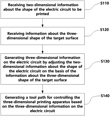
1. A method for printing an electric circuit directly on a target surface having a three-dimensional shape using a three-dimensional printing apparatus, the method comprising:
(a) receiving two-dimensional information about the shape of the electric circuit to be printed;
(b) receiving information about the three-dimensional shape of the target surface;
(c) generating three-dimensional information on the electric circuit to be printed by adjusting the two-dimensional information about the shape of the electric circuit to be printed on the basis of the information about the three-dimensional shape of the target surface; and,
(d) generating a tool path for controlling the three-dimensional printing apparatus based on the three-dimensional information on the electric circuit to be printed which generated in the step (c).
|