| CPC H10N 70/068 (2023.02) [H10N 70/023 (2023.02); H10N 70/046 (2023.02); H10N 70/063 (2023.02); H10N 70/066 (2023.02); H10N 70/245 (2023.02); H10N 70/826 (2023.02); H10N 70/8416 (2023.02); H10N 70/883 (2023.02); H10B 63/30 (2023.02)] | 18 Claims |
|
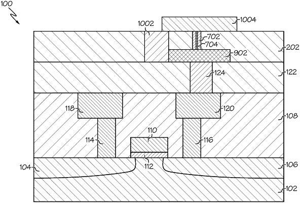
1. A semiconductor structure including at least one memory cell consisting of one transistor and one resistor, the semiconductor structure comprising:
a target metal contact; and
a vertical memory resistive element having first and second electrical contacts, and wherein the vertical memory resistive element comprises dielectric material which is formed in, and fills, a vertically-oriented cell contact hole entirely in a horizontal dielectric layer, and including only one vertically-oriented seam formed in the vertical memory resistive element and surrounded by, and in direct contact with, the dielectric material forming the vertical memory resistive element, and the only one vertically-oriented seam comprising conductive material extending vertically from the first electrical contact to the second electrical contact, one of the first and second electrical contacts being electrically connected to the target metal contact; and
wherein the only one vertically-oriented seam comprises a conductive material selected from any one or more of: a doped mobile element and a doped non-stoichiometric compound including reactive elements, or a combination of previously listed conductive materials.
|