| CPC H10K 59/38 (2023.02) [H10K 50/854 (2023.02); H10K 50/865 (2023.02); H10K 59/12 (2023.02); H10K 71/00 (2023.02)] | 16 Claims |
|
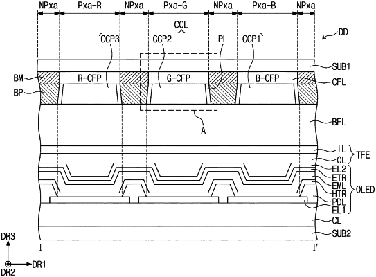
1. A display device comprising:
a display panel having a pixel area and a peripheral area adjacent to the pixel area;
a light control layer disposed on the display panel and at least partially overlapping the pixel area;
a light blocking portion at least partially overlapping the peripheral area; and
a protective layer disposed between the light control layer and the light blocking portion, wherein
the protective layer comprises a plurality of protection patterns, each protection pattern consisting of a single layer,
at least a portion of each of the plurality of protection patterns overlaps the pixel region, and
a spaced portion overlapping the light blocking portion is defined between each of the plurality of protection patterns.
|