| CPC H10K 59/131 (2023.02) [G09G 3/3233 (2013.01); H10K 59/88 (2023.02); G09G 2300/0413 (2013.01); G09G 2300/0426 (2013.01); G09G 2300/0819 (2013.01); G09G 2300/0861 (2013.01); G09G 2310/02 (2013.01)] | 20 Claims |
|
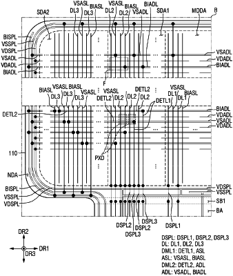
1. A display device comprising:
a substrate comprising a main region and a sub-region protruding from one side of the main region, the main region comprising a display area in which a plurality of emission areas is arranged, and a non-display area disposed around the display area;
a circuit array layer disposed on the substrate and comprising:
a plurality of pixel drivers respectively corresponding to the plurality of emission areas,
data lines configured to transmit data signals to the plurality of pixel drivers,
first dummy lines extending in the same direction as the data lines and respectively adjacent to the data lines, and
second dummy lines extending in a first direction intersecting the data lines; and
a light emitting array layer disposed on the circuit array layer and comprising a plurality of light emitting elements respectively corresponding to the plurality of emission areas,
wherein the display area comprises a middle region adjacent to the sub-region in a second direction which is an extension direction of the data lines, a first side region in contact with the middle region in the first direction, and a second side region between the first side region and the non-display area,
wherein the data lines comprise:
a first data line disposed in the middle region;
a second data line disposed in the first side region; and
a third data line disposed in the second side region,
wherein the first dummy lines comprise a first data detour line disposed in the first side region and adjacent to a part of the second data line, and auxiliary lines other than the first data detour line,
wherein the second dummy lines comprise a second data detour line disposed in the first side region and the second side region and configured to connect the first data detour line to the third data line, and additional lines other than the second data detour line, and
wherein the auxiliary lines comprise:
a bias auxiliary line to which a bias power is configured to be applied; and
a second power auxiliary line to which a second power is configured to be applied, wherein a first power and the second power are for driving the light emitting elements.
|