| CPC H10K 59/121 (2023.02) [G09G 3/3225 (2013.01); H10K 50/80 (2023.02); H10K 59/131 (2023.02); H10K 77/111 (2023.02); H10K 2102/311 (2023.02)] | 20 Claims |
|
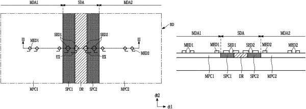
1. A display device comprising:
a substrate including a first main display area, a second main display area, and a sub-display area positioned between the first main display area and the second main display area;
a first driving circuit positioned on the sub-display area of the substrate;
a first sub-pixel circuit and a second sub-pixel circuit positioned on respective sides of the first driving circuit on the sub-display area of the substrate;
a first sub-light-emitting device connected to the first sub-pixel circuit and overlapping the first driving circuit; and
a second sub-light-emitting device connected to the second sub-pixel circuit and overlapping the first driving circuit.
|