| CPC H10K 50/844 (2023.02) [H10K 50/8426 (2023.02); H10K 59/131 (2023.02); H10K 71/00 (2023.02); H10K 59/1201 (2023.02)] | 20 Claims |
|
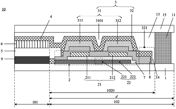
1. A display panel, having a display region and a border region surrounding the display region, wherein the border region comprises a peripheral circuit region and a peripheral region, and the peripheral circuit region is between the display region and the peripheral region; and the display panel comprises:
a base substrate;
a barrier structure, wherein at least a part of the barrier structure is in the peripheral circuit region on the base substrate, and the barrier structure comprises:
an organic barrier layer comprising an opening passing through the organic barrier layer, wherein an extension direction of the opening is substantially same as an extension direction of an edge, close to the opening, of the display panel, in the display panel; and
an inorganic barrier layer covering the organic barrier layer and filling the opening; and
a peripheral circuit in the peripheral circuit region on the base substrate;
an encapsulation substrate on a side, away from the base substrate, of the barrier structure; and
an encapsulation sealant filled between the base substrate and the encapsulation substrate and covering the display region and the peripheral circuit region;
the peripheral circuit comprises a plurality of first signal wires, the plurality of first signal wires are in a same layer and a gap is provided between two adjacent first signal wires of the plurality of the first signal wires, an orthographic projection of the opening on the base substrate is in an orthographic projection of the gap between two adjacent first signal wires of the plurality of the first signal wires on the base substrate, and the orthographic projection of the opening on the base substrate does not overlap with all orthographic projections of the plurality of the first signal wires that are in the same layer on the base substrate.
|