| CPC H10K 50/8423 (2023.02) [H10K 59/122 (2023.02)] | 17 Claims |
|
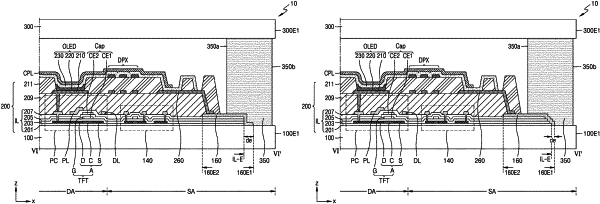
1. A display panel comprising:
a first substrate;
pixels arranged on the first substrate and configured to define a display area;
a thin film transistor (TFT) between the first substrate and the pixels, the TFT being electrically connected to one of the pixels and comprising a semiconductor layer and a gate electrode;
a second substrate facing the first substrate;
an insulating layer comprising a buffer layer between the first substrate and the semiconductor layer and a gate insulating layer between the semiconductor layer and the gate electrode;
a conductive layer on the insulating layer; and
a sealing member between the first substrate and the second substrate and surrounding the display area, and comprising an inner side surface facing the display area, and an outer side surface that is opposite to the inner side surface,
wherein an edge of the insulating layer and an edge of the conductive layer are between the inner side surface and the outer side surface of the sealing member in a plan view, such that a portion of the sealing member adjacent the outer side surface directly contacts the first substrate at the edge of the conductive layer at which the conductive layer directly contacts the first substrate.
|