US 11,937,429 B2
Integrated structures including material containing silicon, nitrogen, and at least one of carbon, oxygen, boron and phosphorus
Justin B. Dorhout, Boise, ID (US); Fei Wang, Boise, ID (US); Chet E. Carter, Boise, ID (US); Ian Laboriante, Boise, ID (US); John D. Hopkins, Meridian, ID (US); Kunal Shrotri, Boise, ID (US); Ryan Meyer, Boise, ID (US); Vinayak Shamanna, Boise, ID (US); Kunal R. Parekh, Boise, ID (US); Martin C. Roberts, Boise, ID (US); and Matthew Park, Boise, ID (US)
Assigned to Micron Technology, Inc., Boise, ID (US)
Filed by Micron Technology, Inc., Boise, ID (US)
Filed on Dec. 20, 2021, as Appl. No. 17/556,704.
Application 17/556,704 is a division of application No. 16/907,967, filed on Jun. 22, 2020, granted, now 11,239,252.
Application 16/907,967 is a continuation of application No. 16/158,039, filed on Oct. 11, 2018, granted, now 10,720,446.
Application 16/158,039 is a continuation of application No. 15/133,119, filed on Apr. 19, 2016, granted, now 10,157,933, issued on Dec. 18, 2018.
Prior Publication US 2022/0115401 A1, Apr. 14, 2022
Int. Cl. H01L 27/1157 (2017.01); H01L 23/528 (2006.01); H01L 23/532 (2006.01); H10B 43/27 (2023.01); H10B 43/35 (2023.01)
CPC H10B 43/27 (2023.02) [H01L 23/528 (2013.01); H01L 23/53257 (2013.01); H10B 43/35 (2023.02)] 18 Claims
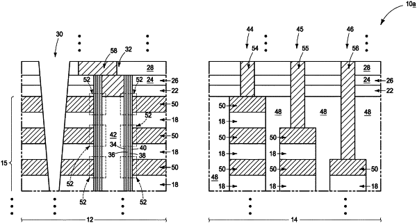
OG exemplary drawing
 
1. A method of forming an integrated structure, comprising:
forming a vertical stack comprising first levels alternating with second levels, the first levels comprising a nitride material and the second levels comprising a dielectric material, an uppermost level of the stack being one of the first levels;
forming an insulative material over the uppermost level of the stack;
forming an etch-resistant material over the insulative material, the etch resistant material comprising silicon, nitrogen, and one or more substances selected from the group consisting of carbon, oxygen, boron and phosphorus, the material being in direct physical contact with the insulative material;
forming an opening extending through the etch resistant material, through the insulative material, and through at least some of the first and second levels;
removing the nitride material of the first levels without removing a remaining region of the etch-resistant material; and
replacing the nitride material with conductive material.