| CPC H05B 45/34 (2020.01) [H04N 23/56 (2023.01); H05B 45/3725 (2020.01); H04N 23/74 (2023.01)] | 4 Claims |
|
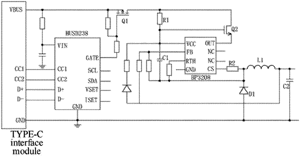
1. A power supply circuit for a fill light, characterized in that said power supply circuit is electrically connected to an external power supply device with a Universal Serial Bus Power Delivery (USB PD) protocol, comprising:
a Universal Serial Bus TYPE-C(USB TYPE-C) interface module for electrically connecting to the external power supply device with the USB PD protocol, wherein said USB TYPE-C interface module includes a communication end and a power supply end;
a Power Delivery (PD) induction module, wherein said PD induction module includes a communication end and a control end, and the communication end of said PD induction module is connected with the communication end of said USB TYPE-C interface module;
a first switching tube (Q1), wherein the gate of said first switching tube (Q1) is connected with the control end of said PD induction module, and the source of said first switching tube (Q1) is connected with the power supply end of said USB TYPE-C interface module; and
a voltage stabilization module, wherein said voltage stabilization module is a Buck-Boost switching power supply module, and the input of said voltage stabilization module is connected with the drain of said first switching tube (Q1),
wherein said voltage stabilization module includes a power supply chip (model BP3208), a first resistor (R1), a second resistor (R2), a first capacitor (C1), a second capacitor (C2), an inductor (L1), a second switching tube (Q2) and a diode (D1), said power supply chip is includes a driving end and a sampling end,
the drain of said first switching tube (Q1) is connected successively to a negative terminal of said diode (D1) through said first resistor (R1) and said first capacitor (C1), a positive terminal of said diode (D1) is grounded, the drain of said second switching tube (Q2) is connected to the drain of said first switching tube (Q1), the gate of said second switching tube(Q2) is connected at the point where said first resistor (R1) is connected to said first capacitor (C1), the source of said second switching tube (Q2) is connected to the driving end of said power supply chip, the negative terminal of said diode (D1) is connected to the sampling end of said power supply chip through said second resistor (R2), the negative terminal of said diode (D1) is connected to one end of said inductor (L1), and the other end of said inductor (L1) is grounded through said second capacitor (C2) and serves as an output of said voltage stabilization module.
|