| CPC H05B 33/22 (2013.01) [H05B 33/04 (2013.01); H05B 33/14 (2013.01)] | 7 Claims |
|
1. A light emitting device comprising:
a substrate;
a light emitting portion positioned over the substrate;
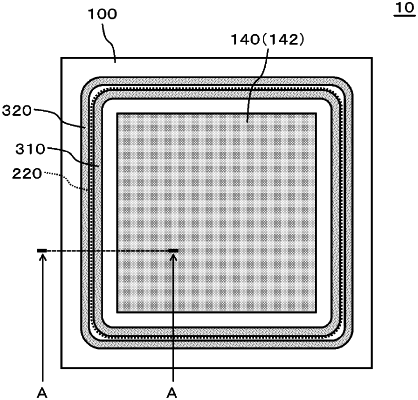
a first structure surrounding a light emitting region comprising the light emitting portion;
a second structure positioned outside the first structure with respect to the light emitting region and surrounding the light emitting region;
a sealing layer covering the light emitting portion, the first structure, and the second structure; and
a resin layer covering at least a portion of the sealing layer overlapping with the light emitting region,
wherein the first structure comprises a first side surface positioned at the light emitting region side, and a second side surface positioned opposite to the first side surface and inclined away from the light emitting region with distance from the substrate, and
wherein the second structure comprises a third side surface positioned at the light emitting region side, and a fourth side surface positioned opposite to the third side surface and inclined away from the light emitting region with distance from the substrate.
|