| CPC H04N 23/54 (2023.01) [H04N 23/57 (2023.01); H05K 1/181 (2013.01); H05K 1/185 (2013.01); H05K 2201/0338 (2013.01); H05K 2201/09409 (2013.01); H05K 2201/10121 (2013.01); H05K 2201/10151 (2013.01); H05K 2201/10969 (2013.01)] | 20 Claims |
|
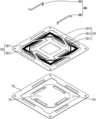
1. A circuit board comprising:
an insulating portion; and
a pattern portion disposed on the insulating portion,
wherein the insulating portion includes:
a first insulating region, and
a second insulating region disposed outside the first insulating region and spaced apart from the first insulating region with a separation region therebetween;
wherein the pattern portion includes:
a first pattern portion for signal transmission; and
a second pattern portion including a dummy pattern separated from the first pattern portion,
wherein the first pattern portion includes:
a first terminal portion disposed on the first insulating region;
a second terminal portion disposed on the second insulating region; and
a connection portion disposed on the separation region and connecting between the first terminal portion and the second terminal portion,
wherein the second pattern portion includes:
a second-first pattern portion disposed on the first insulating region; and
a second-second pattern portion disposed on the second insulating region and separated from the second-first pattern portion.
|