US 11,936,409 B2
Data transmitting and receiving device
Chulwoo Kim, Seoul (KR); Jonghyuck Choi, Suwon-si (KR); Seungwoo Park, Seoul (KR); Hyun Woo Cho, Suwon-si (KR); Tae-Jin Kim, Hwaseong-si (KR); Jae Suk Yu, Seoul (KR); Kil Hoon Lee, Seoul (KR); and Young Hwan Chang, Yongin-si (KR)
Assigned to Samsung Electronics Co., Ltd., (KR); and Korea University Research and Business Foundation, (KR)
Filed by SAMSUNG ELECTRONICS CO., LTD., Suwon-si (KR)
Filed on Mar. 1, 2022, as Appl. No. 17/683,476.
Claims priority of application No. 10-2021-0095707 (KR), filed on Jul. 21, 2021.
Prior Publication US 2023/0026005 A1, Jan. 26, 2023
Int. Cl. H04B 1/04 (2006.01); H04L 25/03 (2006.01)
CPC H04B 1/04 (2013.01) [H04L 25/03057 (2013.01)] 20 Claims
OG exemplary drawing
 
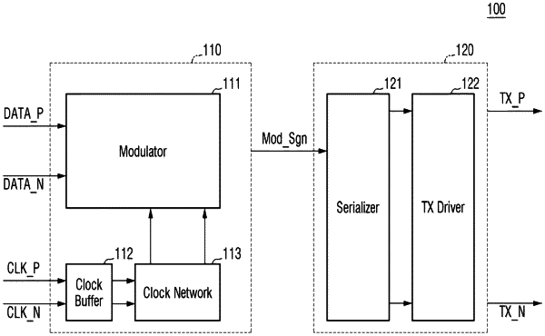
1. A transmitter, comprising:
a processing unit configured to receive a clock signal and a data signal, set a value of a consecutive identical digit (CID) value related to the data signal and generate a modulation signal during a unit interval (UI) based on the data signal and the CID value; and
a transmitter driver configured to output output signals having different voltage levels during the UI by receiving the modulation signal.