| CPC H03K 5/135 (2013.01) [H03K 2005/00019 (2013.01)] | 10 Claims |
|
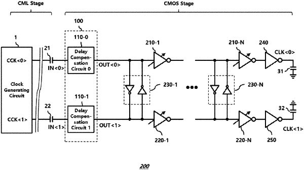
1. A clock transfer circuit comprising:
a first stage circuit configured to produce an output signal that uses a second signaling technology from an input signal that uses a first signaling technology; and
a second stage circuit configured to produce a clock signal by delaying the output signal;
wherein the first stage circuit includes a semiconductor device configured to compensate for delay fluctuation caused by fluctuation of power supply voltage between a first power source and a second power source.
|