US 11,936,299 B2
Transistor having asymmetric threshold voltage and buck converter
Chu Fu Chen, Zhubei (TW); Chi-Feng Huang, Zhubei (TW); Chia-Chung Chen, Keelung (TW); Chin-Lung Chen, Zhubei (TW); Victor Chiang Liang, Hsinchu (TW); and Chia-Cheng Pao, Hsinchu (TW)
Assigned to TAIWAN SEMICONDUCTOR MANUFACTURING COMPANY, LTD., Hsinchu (TW)
Filed by TAIWAN SEMICONDUCTOR MANUFACTURING COMPANY, LTD., Hsinchu (TW)
Filed on Sep. 21, 2020, as Appl. No. 17/027,032.
Application 17/027,032 is a continuation of application No. 15/938,482, filed on Mar. 28, 2018, granted, now 10,784,781, issued on Sep. 22, 2020.
Claims priority of provisional application 62/591,871, filed on Nov. 29, 2017.
Prior Publication US 2021/0028309 A1, Jan. 28, 2021
This patent is subject to a terminal disclaimer.
Int. Cl. H02M 3/158 (2006.01); H01L 21/84 (2006.01); H01L 29/08 (2006.01); H01L 29/423 (2006.01); H01L 29/66 (2006.01); H01L 29/78 (2006.01); H01L 29/80 (2006.01); H01L 21/265 (2006.01)
CPC H02M 3/1582 (2013.01) [H01L 21/84 (2013.01); H01L 29/0847 (2013.01); H01L 29/4232 (2013.01); H01L 29/66659 (2013.01); H01L 29/7835 (2013.01); H01L 29/7836 (2013.01); H01L 29/80 (2013.01); H01L 21/26586 (2013.01); H02M 3/158 (2013.01)] 20 Claims
OG exemplary drawing
 
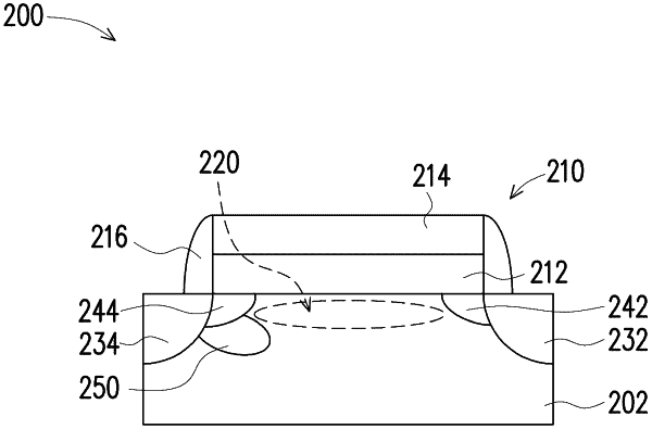
1. A transistor comprising:
a gate structure over a substrate, wherein the substrate includes a channel region;
a source/drain (S/D) in the substrate adjacent to the gate structure;
a lightly doped drain (LDD) region adjacent to the S/D, wherein a dopant concentration in the LDD region is less than a dopant concentration in the S/D; and
a doping extension region adjacent the LDD region, wherein the doping extension region extends farther under the gate structure than the LDD region, and a maximum depth of the doping extension region is 10-times to 30-times greater than a maximum depth of the LDD.