| CPC H02M 3/157 (2013.01) [H02M 1/0003 (2021.05); H02M 3/1566 (2021.05); H02M 3/1584 (2013.01); H02M 3/1586 (2021.05); H03M 1/502 (2013.01)] | 16 Claims |
|
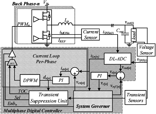
1. A mixed-signal controller for controlling a multiphase average-current-mode voltage regulator having an output connected to a load, said controller comprises:
a. a digital voltage-sampling Analog-to-Digital Converter (ADC), based on Delay-Lines (DLs) and configured to obtain a sample of an output voltage signal and to convert said output voltage signal from analog to digital representation;
b. a digital current-sampling ADC, based on Delay-Lines (DLs) and configured to obtain a sample of a per-phase inductor current and to convert said inductor current from analog to digital representation;
c. a digital compensator, for voltage regulation, receiving as input a digital voltage error signal (ve[n]) created by a voltage loop and configured to generate a current reference signal, based on said digital voltage error signal;
d. a digital compensator for current regulation, for receiving as input a current error signal ie[n] and for generating a duty-ratio command signal, based on said digital current error signal;
e. a multiphase Digital Pulse Width Modulator (DPWM) , based on DLs, for receiving as input the duty-ratio command signal for each phase, for generating a pulse-width-modulated signal (for each phase) that is fed to the gates of transistors of said ADC, to thereby control per-phase currents and output voltage supplied to said load;
f. an analog front-end, for receiving differential measurements of the output voltage and the per-phase inductor current, where each signal is converted to a single-ended representation, such that single-ended signals are used for steady-state control via ADC measurement and a single-ended output voltage is used for transient detection and output voltage extremum detection during transient;
g. a Transient Suppression Unit (TSU), for receiving as input a digital indication signal from the analog front-end and for generating gating signals being fed to the gates of transistors of a converter during a transient event, to thereby control the current and voltage supplied to said load during said transient event;
h. a Phase Count Optimizer (PCO) unit for receiving as input a digital current reference signal and for generating, for each phase, an enable/disable control signal to a corresponding output tri-state buffer; and
i. an Active Voltage Positioning (AVP) unit for receiving as input a digital current reference signal and for generating a voltage loop compensator voltage reference signal.
|