| CPC H02M 3/075 (2021.05) [G11C 5/145 (2013.01); H02M 1/009 (2021.05); H02M 3/155 (2013.01)] | 12 Claims |
|
1. A charge pump circuit comprising:
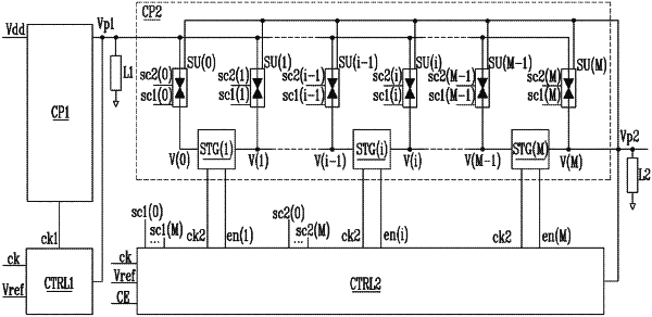
a first charge pump including an input terminal configured for receiving a supply voltage, the first charge pump configured to boost the received supply voltage to provide at an output terminal of the first charge pump a first charge pump voltage; and
a second charge pump including an input terminal coupled to the output terminal of the first charge pump and configured for receiving the first charge pump voltage, the second charge pump configured to boost the received first charge pump voltage to provide at an output terminal of the second charge pump a second charge pump voltage, wherein:
the second charge pump comprises a sequence of charge pump stages connected in series between the input and output terminals of the second charge pump, each charge pump stage being configured to be selectively enabled to boost an input stage voltage at a stage input terminal by a voltage corresponding to the supply voltage to provide at a stage output terminal a corresponding output stage voltage when the charge pump stage is enabled,
each charge pump stage is configured to be selectively disabled to bring its corresponding stage output terminal to a high impedance state and is associated with a corresponding bypass unit comprising a first transistor configured to electrically couple the stage output terminal to the output terminal of the first charge pump when the charge pump stage is disabled, the bypass unit further comprising a second transistor connected in parallel to the first transistor and being configured to be activated when the charge pump stage is disabled, and
the charge pump circuit further comprises a voltage drop sensing device configured to detect drops in the first charge pump voltage and to deactivate the second transistors of the bypass unit associated to the disabled charge pump stages when a drop in the first charge pump voltage is detected.
|