| CPC H01Q 21/28 (2013.01) [H01Q 1/24 (2013.01); H01Q 9/0407 (2013.01); H01Q 21/0006 (2013.01); H04B 1/40 (2013.01)] | 15 Claims |
|
1. An electronic device comprising:
a housing comprising a first plate, a second plate facing away from the first plate, and a side wall surrounding a space between the first plate and the second plate, and coupled to the second plate or integrally formed with the second plate;
a display visible through at least a portion of the first plate;
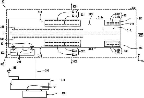
an antenna structure disposed within the housing, the antenna structure comprising:
a printed circuit board comprising a first surface extending in a first direction and a second surface extending in a second direction opposite to the first direction;
a first area comprising a first antenna array comprising a plurality of first antenna elements formed within the printed circuit board or on the first surface;
a second area comprising a second antenna array comprising a plurality of second antenna elements formed closer to the second surface than the plurality of first antenna elements within the printed circuit board, or on the second surface, wherein when viewed from above the first surface, the second area at least partially overlaps the first area;
a third area comprising a third antenna array comprising a plurality of third antenna elements formed within the printed circuit board or on the first surface, wherein when viewed from above the first surface, the third area does not overlap the first area;
a fourth area comprising a fourth antenna array comprising a plurality of fourth antenna elements formed closer to the second surface than the plurality of third antenna elements within the printed circuit board, or on the second surface, wherein when viewed from above the first surface, the fourth area at least partially overlaps the third area; and
a ground layer disposed between the first antenna array and the second antenna array within the printed circuit board, wherein when viewed from above the first surface, the ground layer at least partially overlaps the first area and the second area; and
at least one wireless communication circuit electrically connected to the first antenna array, the second antenna array, the third antenna array and the fourth antenna array, and configured transmit and/or receive a signal having a frequency in a range of about 3 GHz to 100 GHz.
|