| CPC H01L 33/382 (2013.01) [H01L 27/156 (2013.01); H01L 33/0093 (2020.05); H01L 33/62 (2013.01); H01L 2933/0016 (2013.01); H01L 2933/0066 (2013.01)] | 12 Claims |
|
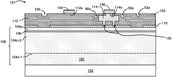
1. A light emitting diode (LED) array comprising:
a light-emitting pixel area integral to a monolithic body, the light-emitting pixel area including semiconductor layers comprising: a second portion of an N-type layer, an active region, and a P-type layer;
the monolithic body comprising a first portion of an N-type layer, the second portion of the N-type layer being integral to the first portion of the N-type layer;
a plurality of anodes, each anode comprising a P-contact layer and one or more P-contact materials, each P-contact layer being in contact with the P-type layer;
a common cathode comprising one or more N-contact materials in contact with the first portion of the N-type layer;
one or more dielectric materials insulating: the second portion of the N-type layer, the active region, and the P-type layer from the common cathode; the plurality of anodes from each other; and the plurality of anodes from the common cathode.
|