| CPC H01L 31/055 (2013.01) [H01L 25/167 (2013.01); H01L 31/022408 (2013.01); H01L 31/03046 (2013.01); H01L 31/101 (2013.01); H01L 31/125 (2013.01)] | 20 Claims |
|
1. A photo-detecting device, comprising:
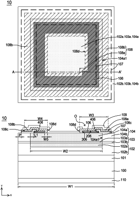
a substrate (100);
a first semiconductor layer (101) located on the substrate (100) and having a first dopant;
a second semiconductor layer (104) located on the first semiconductor layer (101) and having a first region (104a) and a second region (104b), wherein the first region (104a) has a first perimeter (104a1) and comprises a second dopant and a third dopant, and the second region (104b) comprises the second dopant and does not comprise the third dopant;
a light-absorbing layer (102) located between the first semiconductor layer (101) and the second semiconductor layer (104), and having a third region (102a) and a fourth region (102b), wherein the third region (102a) comprises the third dopant, and the fourth region (102b) does not comprise the third dopant; and
a semiconductor contact layer (106) contacting the first region; and
an electrode structure (108) located on the semiconductor contact layer (106) and having an outer sidewall (108c) aligned with the first perimeter (104a1),
wherein the semiconductor contact layer 006) has a first thickness greater than 50 Å and smaller than 1000 Å, and
wherein the second semiconductor layer (104) further comprises a fifth region (104c) located between the first region (104a) and the second region (104b), and the fifth region (104c) comprises the third dopant and is located beyond the outer sidewall (108c) in a horizontal direction.
|