| CPC H01L 31/035218 (2013.01) [H01L 31/022408 (2013.01); H01L 31/03048 (2013.01); H01L 31/0312 (2013.01); H01L 31/0324 (2013.01); H01L 31/0336 (2013.01); H01L 31/07 (2013.01); H01L 31/108 (2013.01); H01L 31/18 (2013.01); H01L 31/1848 (2013.01); H10K 30/00 (2023.02)] | 16 Claims |
|
1. A method for producing a photovoltaic junction, the method comprising:
applying a metallic contact to a first surface area of a semiconductor layer to form a first physical junction between a first surface area of the metallic contact and the first surface area of the semiconductor layer, the first physical junction forming a Schottky diode;
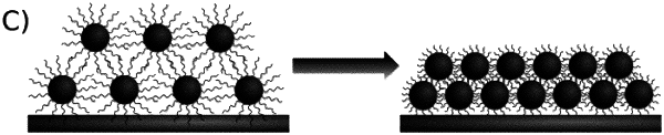
coating a second surface area of the semiconductor layer and a second surface area of the metallic contact with a composition including a plurality of ligand-protected quantum dots;
carrying out a ligand-exchange with the ligand-protected quantum dots to form a light absorbing layer, wherein a second physical junction exists between a first surface area of the light absorbing layer and the second surface area of the semiconductor layer and a third physical junction exists between a second surface area of the light absorbing layer and the second surface area of the metallic contact, the second physical junction forming a diode that exhibits Shockley-Read Hall trap-assisted recombination, and the third physical junction forming an ohmic contact; wherein
the photovoltaic junction exhibits absorption across one or more wavelengths in the range from about 200 nm to about 2000 nm.
|