| CPC H01L 29/41741 (2013.01) [H01L 29/401 (2013.01); H01L 29/42392 (2013.01); H01L 29/66666 (2013.01); H01L 29/7827 (2013.01)] | 20 Claims |
|
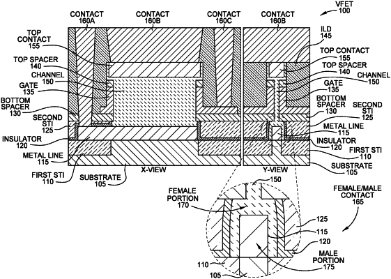
1. A vertical field-effect transistor (VFET) comprising:
a vertical channel;
a top conductive contact for one of a drain or source region, wherein a top end of the vertical channel wraps around the top conductive contact; and
a bottom conductive contact disposed on a substrate for one of a drain or source region, wherein a bottom end of the vertical channel wraps around the bottom conductive contact, and wherein the bottom end of the vertical channel and the bottom conductive contact both directly contact the substrate.
|