| CPC H01L 29/1033 (2013.01) [H01L 21/823807 (2013.01); H01L 21/823814 (2013.01); H01L 21/823871 (2013.01); H01L 27/092 (2013.01); H01L 29/0847 (2013.01); H01L 29/16 (2013.01); H01L 29/41775 (2013.01); H01L 29/42364 (2013.01); H01L 29/42372 (2013.01)] | 19 Claims |
|
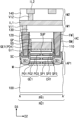
1. A semiconductor device, comprising:
a substrate including a first region and a second region;
a first active pattern on the first region, the first active pattern including a pair of first source/drain patterns and a first channel pattern between ones of the pair of first source/drain patterns, the first source/drain patterns being spaced apart in a first direction, the first channel pattern including a plurality of first semiconductor patterns stacked on the substrate;
a second active pattern on the second region, the second active pattern including a pair of second source/drain patterns and a second channel pattern between ones the pair of second source/drain patterns, the second channel pattern including a plurality of second semiconductor patterns stacked on the substrate;
a support pattern between two vertically adjacent ones of the plurality of first semiconductor patterns, the support pattern connecting the two vertically adjacent first semiconductor patterns to each other; and
a first gate electrode and a second gate electrode on the first channel pattern and the second channel pattern, respectively,
wherein a length of the first channel pattern is greater than a length of the second channel pattern,
a ratio of a width of the support pattern to the length of the first channel pattern is in a range of about 0.05 to about 0.2, and
wherein the first gate electrode includes a first segment and a second segment that are between the two vertically adjacent first semiconductor patterns, and the support pattern is between the first segment and the second segment in the first direction.
|