| CPC H01L 27/14612 (2013.01) [H01L 27/14636 (2013.01); H01L 27/14638 (2013.01); H01L 27/14641 (2013.01); H01L 27/14643 (2013.01); H01L 27/14683 (2013.01)] | 19 Claims |
|
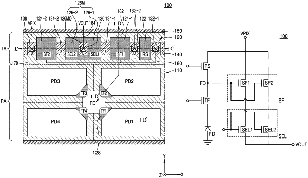
1. An image sensor, comprising:
a plurality of unit pixels, wherein each of the plurality of unit pixels includes
a photodiode;
a transfer transistor connected between the photodiode and a floating diffusion area;
a reset transistor connected between a source voltage node and the floating diffusion area;
a selection transistor; and
at least two source follower transistors between the source voltage node and the selection transistor, each of the at least two source follower transistors having a gate connected to the floating diffusion area,
wherein the selection transistor is between the at least two source follower transistors and an output voltage node,
wherein the at least two source follower transistors are electrically connected between the source voltage node and the selection transistor in parallel such that
the image sensor is configured to cause a voltage to be applied from the source voltage node to the selection transistor through each of the at least two source follower transistors in parallel.
|