US 11,935,891 B2
Non-silicon N-type and P-type stacked transistors for integrated circuit devices
Gilbert Dewey, Beaverton, OR (US); Patrick Morrow, Portland, OR (US); Ravi Pillarisetty, Portland, OR (US); Rishabh Mehandru, Portland, OR (US); Cheng-ying Huang, Hillsboro, OR (US); Willy Rachmady, Beaverton, OR (US); and Aaron Lilak, Beaverton, OR (US)
Assigned to Intel Corporation, Santa Clara, CA (US)
Filed by Intel Corporation, Santa Clara, CA (US)
Filed on Jun. 13, 2022, as Appl. No. 17/839,338.
Application 17/839,338 is a continuation of application No. 16/957,664, granted, now 11,387,238, previously published as PCT/US2018/020612, filed on Mar. 2, 2018.
Prior Publication US 2022/0310605 A1, Sep. 29, 2022
This patent is subject to a terminal disclaimer.
Int. Cl. H01L 27/092 (2006.01); H01L 21/8238 (2006.01); H01L 25/07 (2006.01); H01L 27/06 (2006.01); H01L 29/06 (2006.01); H01L 29/778 (2006.01); H01L 29/78 (2006.01)
CPC H01L 27/0924 (2013.01) [H01L 21/823807 (2013.01); H01L 25/074 (2013.01); H01L 27/0688 (2013.01); H01L 29/0669 (2013.01); H01L 29/7782 (2013.01); H01L 29/785 (2013.01)] 20 Claims
OG exemplary drawing
 
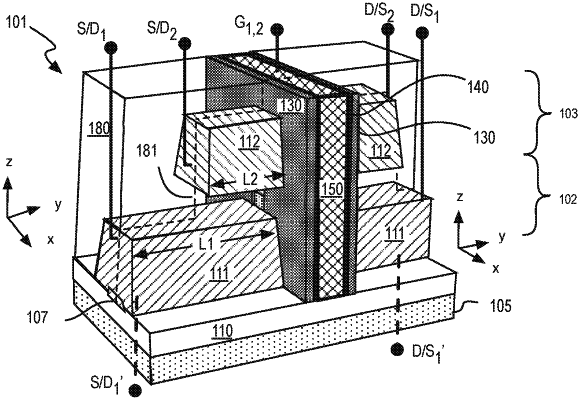
1. An integrated circuit (IC) structure, comprising:
a material stack including a first channel material and a second channel material, wherein the first channel material comprises Ge and the second channel material comprises one or more Group III elements and one or more Group V elements;
one or more gate electrodes adjacent to a sidewall of the first and second channel materials; and
source and drain terminals coupled to the first and second channel materials.