US 11,935,857 B2
Surface finishes with low RBTV for fine and mixed bump pitch architectures
Kristof Darmawaikarta, Chandler, AZ (US); Robert May, Chandler, AZ (US); Sashi Kandanur, Phoenix, AZ (US); Sri Ranga Sai Boyapati, Chandler, AZ (US); Srinivas Pietambaram, Chandler, AZ (US); Steve Cho, Chandler, AZ (US); Jung Kyu Han, Chandler, AZ (US); Thomas Heaton, Mesa, AZ (US); Ali Lehaf, Phoenix, AZ (US); Ravindranadh Eluri, Chandler, AZ (US); Hiroki Tanaka, Chandler, AZ (US); Aleksandar Aleksov, Chandler, AZ (US); and Dilan Seneviratne, Chandler, AZ (US)
Assigned to Intel Corporation, Santa Clara, CA (US)
Filed by Intel Corporation, Santa Clara, CA (US)
Filed on Sep. 23, 2022, as Appl. No. 17/952,080.
Application 17/952,080 is a division of application No. 16/177,022, filed on Oct. 31, 2018, granted, now 11,488,918.
Prior Publication US 2023/0015619 A1, Jan. 19, 2023
Int. Cl. H01L 21/00 (2006.01); H01L 21/768 (2006.01); H01L 23/00 (2006.01); H01L 23/522 (2006.01)
CPC H01L 24/17 (2013.01) [H01L 21/76877 (2013.01); H01L 21/76897 (2013.01); H01L 23/5226 (2013.01); H01L 24/09 (2013.01); H01L 24/11 (2013.01); H01L 2924/01029 (2013.01); H01L 2924/0105 (2013.01)] 22 Claims
OG exemplary drawing
 
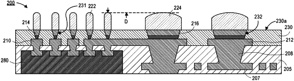
1. A method of forming an electronic package, comprising:
embedding a bridge substrate in a packaging substrate;
forming first vias to the bridge substrate;
forming second vias to electrical routing in the packaging substrate;
forming first conductive pads over the first vias, wherein the first conductive pads have a first surface area; and
forming second conductive pads over the second vias, wherein the second conductive pads have a second surface area that is greater than the first surface area.