| CPC H01L 24/17 (2013.01) [H01L 21/56 (2013.01); H01L 21/568 (2013.01); H01L 23/3135 (2013.01); H01L 24/19 (2013.01); H01L 24/85 (2013.01); H01L 25/105 (2013.01); H01L 23/5389 (2013.01); H01L 24/13 (2013.01); H01L 24/16 (2013.01); H01L 24/32 (2013.01); H01L 24/48 (2013.01); H01L 24/73 (2013.01); H01L 24/81 (2013.01); H01L 24/92 (2013.01); H01L 2224/0401 (2013.01); H01L 2224/04042 (2013.01); H01L 2224/04105 (2013.01); H01L 2224/12105 (2013.01); H01L 2224/131 (2013.01); H01L 2224/13147 (2013.01); H01L 2224/16225 (2013.01); H01L 2224/32225 (2013.01); H01L 2224/45099 (2013.01); H01L 2224/48091 (2013.01); H01L 2224/48227 (2013.01); H01L 2224/73204 (2013.01); H01L 2224/73253 (2013.01); H01L 2224/73267 (2013.01); H01L 2224/81005 (2013.01); H01L 2224/81203 (2013.01); H01L 2224/81815 (2013.01); H01L 2224/85 (2013.01); H01L 2224/92125 (2013.01); H01L 2225/1011 (2013.01); H01L 2225/1023 (2013.01); H01L 2225/1035 (2013.01); H01L 2225/1041 (2013.01); H01L 2225/1058 (2013.01); H01L 2225/107 (2013.01); H01L 2924/00012 (2013.01); H01L 2924/00014 (2013.01); H01L 2924/12042 (2013.01); H01L 2924/15311 (2013.01); H01L 2924/15331 (2013.01); H01L 2924/181 (2013.01); H01L 2924/18161 (2013.01); H01L 2924/18162 (2013.01); H01L 2924/19107 (2013.01); H01L 2924/3511 (2013.01)] | 14 Claims |
|
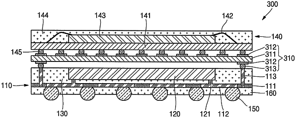
1. A semiconductor device comprising:
a first redistribution layer comprising a first dielectric and a first conductive layer;
a semiconductor die mounted to and electrically connected to an upper side of the first redistribution layer, where the semiconductor die comprises a die bonding pad on a lower die side of the semiconductor die and over the upper side of the first redistribution layer, and where the die bonding pad electrically connects the semiconductor die to the first conductive layer of the first redistribution layer;
a lower encapsulant that covers a lower side of the first dielectric;
a conductive pillar on the first redistribution layer, where a lower end of the conductive pillar is electrically connected to the first conductive layer of the first redistribution layer, and the lower end of the conductive pillar is vertically lower than the die bonding pad;
an upper encapsulant that encapsulates the upper side of the first redistribution layer, the conductive pillar, and the semiconductor die, where the upper encapsulant comprises an upper encapsulant side facing away from the first redistribution layer and a lower encapsulant side facing toward the first redistribution layer;
a second conductive layer on the upper encapsulant side, where the second conductive layer is electrically connected to the first conductive layer of the first redistribution layer through the conductive pillar; and
a material underfilling directly vertically between the semiconductor die and the first redistribution layer,
wherein:
a first lateral side of the lower encapsulant is coplanar with a first lateral side of the upper encapsulant; and
a first lateral side of the first redistribution layer is coplanar with the first lateral side of the upper encapsulant.
|