| CPC H01L 23/642 (2013.01) [H01L 29/401 (2013.01); H01L 29/41708 (2013.01); H01L 29/41741 (2013.01); H01L 29/41775 (2013.01); H01L 29/6634 (2013.01); H01L 29/7398 (2013.01)] | 15 Claims |
|
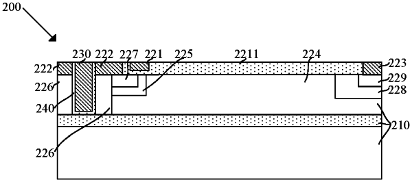
1. A semiconductor device, comprising:
a silicon substrate, wherein an emitter, a gate, and a collector are formed on the silicon substrate;
a bootstrap electrode, formed on the silicon substrate; and
an insulating layer, formed on the silicon substrate and disposed between the emitter and the bootstrap electrode; wherein a bootstrap capacitor is formed between the emitter and the bootstrap electrode, wherein a groove is defined on the silicon substrate, the insulating layer is formed on an inner wall of the groove, and the bootstrap electrode is disposed in the groove.
|