| CPC H01L 23/544 (2013.01) [H01L 21/02389 (2013.01); H01L 21/823431 (2013.01); H01L 27/0886 (2013.01); H01L 29/66795 (2013.01); H01L 29/785 (2013.01); H01L 2223/54426 (2013.01)] | 21 Claims |
|
1. A method of forming an alignment mark array, the method comprising:
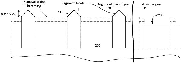
providing a III-V compound substrate having a device region and an alignment mark region, wherein the III-V compound substrate is characterized by a processing surface;
forming a hardmask layer having a first set of openings on the alignment mark region exposing a first surface portion of the processing surface of the III-V compound substrate and a second set of openings on the device region exposing a second surface portion of the processing surface of the III-V compound substrate, wherein each of the first set of openings corresponds to an alignment mark of the alignment mark array;
etching the first surface portion and the second surface portion of the III-V compound substrate using the hardmask layer as a mask to form a plurality of trenches; and
epitaxially regrowing a semiconductor layer in the trenches to form the alignment marks extending to a predetermined height over the processing surface of the III-V compound substrate.
|