| CPC H01L 23/535 (2013.01) [H01L 21/76826 (2013.01); H01L 21/76829 (2013.01); H01L 21/76895 (2013.01); H01L 21/76897 (2013.01); H01L 21/823431 (2013.01); H01L 21/823475 (2013.01); H01L 21/845 (2013.01); H01L 27/088 (2013.01); H01L 27/0886 (2013.01); H01L 27/1211 (2013.01); H01L 29/0649 (2013.01); H01L 29/0847 (2013.01); H01L 29/41791 (2013.01); H01L 29/66545 (2013.01); H01L 29/785 (2013.01); H01L 21/76831 (2013.01); H01L 21/76889 (2013.01); H01L 21/823481 (2013.01)] | 14 Claims |
|
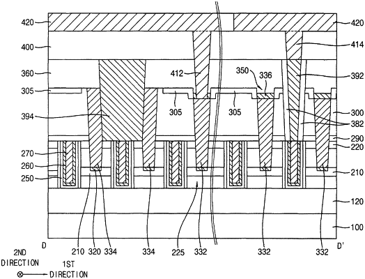
1. A method of manufacturing a semiconductor device, the method comprising:
forming transistors on a substrate such that each of the transistors includes a gate structure and a source/drain layer adjacent thereto;
forming a first insulating interlayer on the substrate to cover the transistors;
forming first contact plugs and a second contact plug through the first insulating interlayer to contact the source/drain layers, respectively;
forming a second insulating interlayer on the first insulating interlayer, and the first and second contact plugs;
forming first and second openings through the first and second insulating interlayers such that the first opening exposes one of the gate structures and the second opening commonly exposes at least one of the gate structures and the second contact plug adjacent thereto;
forming a first insulating spacer on a sidewall of the first opening; and
forming third and fourth contact plugs in the first and second openings, respectively.
|