| CPC H01L 23/528 (2013.01) [H01L 21/38 (2013.01); H01L 21/768 (2013.01)] | 20 Claims |

|
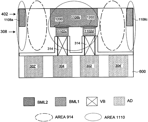
1. An integrated circuit comprising a cell, comprising:
a substrate having a frontside of the substrate and a backside of the substrate;
a device formed in the substrate;
a first active diffusion (AD) region formed in the backside of the substrate;
a second AD region formed in the backside of the substrate and adjacent the first AD region;
a frontside conductive layer formed over the frontside of the substrate and electrically connected to the device;
a first backside conductive layer formed over the backside of the substrate and comprising a first plurality of conductive segments; and
a second backside conductive layer formed over the first backside conductive layer, the second backside conductive layer comprising a second plurality of conductive segments wherein:
the first plurality of conductive segments and the second plurality of conductive segments cover the first AD region from directly above the second backside conductive layer and define an opening directly above the second AD region such that the second AD region is exposed from above the second backside conductive layer; and
the second AD region that is exposed comprises an output region of the cell that is detectable with at least one of a laser, an emission microscopy, or an electron beam from above the second backside conductive layer.
|