| CPC H01L 21/7682 (2013.01) [H01L 21/7624 (2013.01); H01L 21/76804 (2013.01); H01L 21/76805 (2013.01); H01L 23/5226 (2013.01); H01L 23/5329 (2013.01); H01L 29/41733 (2013.01); H01L 29/66439 (2013.01); H01L 29/66742 (2013.01); H01L 21/30604 (2013.01); H01L 29/0673 (2013.01); H01L 29/0847 (2013.01); H01L 29/42392 (2013.01); H01L 29/45 (2013.01); H01L 29/78696 (2013.01)] | 20 Claims |
|
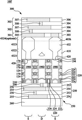
1. A method of forming a semiconductor device, the method comprising:
etching a recess in a substrate, wherein the substrate comprises a first material;
forming a plug in the recess in the substrate, wherein the plug comprises a second material different than the first material;
forming an epitaxial structure over the plug;
forming a gate structure on a first side of the substrate adjacent epitaxial structure;
removing at least a portion of a backside of the substrate to expose the plug;
forming a dielectric layer over the plug, the dielectric layer having an air gap therein;
removing the plug to form a backside via opening through the dielectric layer; and
forming a backside via in the backside via opening, wherein the backside via is electrically coupled to the epitaxial structure.
|