| CPC H01L 21/28158 (2013.01) [H01L 21/02126 (2013.01); H01L 21/02164 (2013.01); H01L 21/02167 (2013.01); H01L 21/0217 (2013.01); H01L 21/022 (2013.01); H01L 21/02208 (2013.01); H01L 21/02211 (2013.01); H01L 21/02274 (2013.01); H01L 21/76224 (2013.01)] | 20 Claims |
|
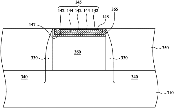
1. A device comprising:
a gate structure over a substrate;
an interlayer dielectric (ILD) layer over the substrate and laterally surrounding the gate structure;
a gate spacer between the gate structure and the ILD layer; and
a dielectric cap over the gate structure and comprising:
a first dielectric layer comprising a first portion extending along a top surface of the gate structure and a second portion extending along an inner sidewall of the gate spacer, wherein the first dielectric layer is a first nitrogen-rich layer on and in contact with the gate structure;
a second dielectric layer comprising a first portion extending along the first portion of the first dielectric layer and a second portion extending along the second portion of the first dielectric layer, wherein the second dielectric layer is a first oxygen-rich layer on and in contact with the first nitrogen-rich layer;
a third dielectric layer over the first oxygen-rich layer, wherein the third dielectric layer is a second nitrogen-rich layer on and in contact with the first oxygen-rich layer;
a fourth dielectric layer over the second nitrogen-rich layer, wherein the fourth dielectric layer is a second oxygen-rich layer on and in contact with the second nitrogen-rich layer; and
a fifth dielectric layer over the fourth dielectric layer, wherein the fifth dielectric layer is thinner than the second dielectric layer.
|