| CPC H01F 10/3254 (2013.01) [H01F 1/0063 (2013.01); H01F 10/3272 (2013.01); H01F 10/329 (2013.01); H10B 61/22 (2023.02); H10N 50/10 (2023.02); H10N 50/80 (2023.02); G11C 11/161 (2013.01); H10N 50/85 (2023.02)] | 20 Claims |
|
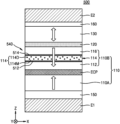
1. A magnetic device comprising:
a fixed layer having perpendicular magnetic anisotropy (PMA) and including a fixed pattern, a free layer having PMA, and a tunnel barrier between the fixed layer and the free layer, wherein the fixed pattern comprises:
a first magnetic pattern;
a second magnetic pattern; and
a hybrid spacer, including a nonmagnetic material layer, between the first magnetic pattern and the second magnetic pattern, the nonmagnetic material layer including a plurality of magnetic nanoparticles dispersed therein, the plurality of magnetic nanoparticles having sizes in a range from about 0.001 nm to about 2 nm.
|