| CPC G11C 29/10 (2013.01) [G11C 7/06 (2013.01); G11C 7/106 (2013.01); G11C 7/1096 (2013.01)] | 17 Claims |
|
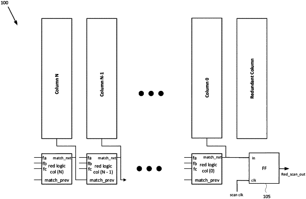
1. A memory, comprising:
a plurality of columns, each column including:
a bit line;
a complement bit line;
a first read multiplexer transistor coupled to the bit line and having a read terminal;
a second read multiplexer transistor coupled to the complement bit line and having a complement read terminal;
a write driver having a write data output terminal and a complement write data output terminal;
a scan multiplexer configured to respond to a scan mode signal to select between a first pair of input terminals coupled to the write data output terminal and the complement write data output terminal and a second pair of input terminals coupled to the read terminal and the complement read terminal; and
a sense amplifier coupled to an output from the scan multiplexer.
|