| CPC G11C 11/4078 (2013.01) [G11C 29/08 (2013.01); H01L 27/0251 (2013.01)] | 19 Claims |
|
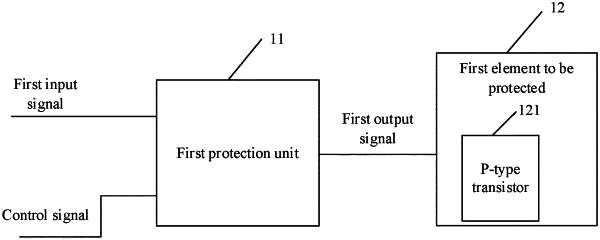
1. A protection circuit applied in a chip, comprising:
a first protection unit, wherein the first protection unit is configured to receive a first input signal and a control signal, and is configured to output a first output signal; and
a first element to be protected comprising a first P-type transistor, wherein a gate of the first P-type transistor is configured to receive the first output signal;
wherein when the chip enters a burn-in test, the first output signal is a high-level signal,
wherein the protection circuit further comprises: a second protection unit and a second element to be protected,
wherein the second protection unit is configured to receive a second input signal and the control signal, and is configured to output a second output signal;
the second element to be protected comprises a second P-type transistor, and a gate of the second P-type transistor is configured to receive the second output signal; and
when the chip enters the burn-in test, the second output signal is a high-level signal.
|