| CPC G09G 3/006 (2013.01) [G09G 3/3233 (2013.01); G09G 2300/0842 (2013.01); G09G 2320/0242 (2013.01); G09G 2330/08 (2013.01); G09G 2330/12 (2013.01)] | 18 Claims |
|
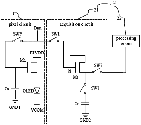
1. A detection circuit for a pixel circuit, wherein the pixel circuit comprises a driving transistor, and a pixel switching unit connected between a control end of the driving transistor and a data signal terminal, the data signal terminal being configured to provide a data signal; and the detection circuit comprises:
an acquisition circuit comprising a test transistor and an energy storage element, wherein a control end of the test transistor is configured to be coupled to the data signal terminal, a first end of the test transistor is configured to be written with a detection signal, and a second end of the test transistor is coupled to the energy storage element; and a structural characteristic of the test transistor is identical to a structural characteristic of the driving transistor; and
a processing circuit coupled to the second end of the test transistor, and configured to detect a voltage at the second end of the test transistor as a detection voltage and regulate the data signal according to the detection voltage;
wherein the acquisition circuit further comprises:
a first switching unit connected between the control end of the test transistor and the data signal terminal;
a second switching unit connected between the second end of the test transistor and the energy storage element; and
a third switching unit connected between the second end of the test transistor and the processing circuit.
|