| CPC G06N 3/0675 (2013.01) [G06N 3/049 (2013.01)] | 9 Claims |
|
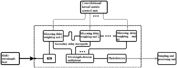
1. A two-dimensional photonic neural network convolutional acceleration chip based on series connection structure, which is integrated with a modulator, M microring delay weighting units, M−1 secondary delay waveguide, a wavelength-division multiplexer and a photodetector; wherein,
the modulator comprises an electrical input port, an optical input port and an optical output port, the optical input port of the modulator is used as the optical input port of the entire chip, and the optical input port of the modulator is used to receive a multi-wavelength optical signal; the optical output port of the modulator is connected to the optical input port of a first microring delay weighting unit; the electrical input port of the modulator is used to receive the signal to be convolved, and the modulator is used to modulate the signal to be convolved into the multi-wavelength optical signal, obtaining a multi-wavelength modulated optical signal containing M×N sub-modulated optical signals;
each of the microring delay weighting unit is comprised of a straight-through waveguide, a coupled waveguide and N microring resonators, the N microring resonators are connected in series through the straight-through waveguide and the coupled waveguide; wherein the input port of the straight-through waveguide is used as the optical input port of the microring delay weighting unit, the output port of the coupled waveguide and the output port of the straight-through waveguide are respectively used as two optical output ports of the microring delay weighting unit; M microring delay weighting units are connected in series through M−1 secondary delay waveguides, the input port of the secondary delay waveguide is connected to the output port of the straight-through waveguide in the microring delay weighting unit before the secondary delay waveguide, and the output port of the secondary delay waveguide is connected to the input port of the straight-through waveguide in the microring delay weighting unit after the secondary delay waveguide; the coupling coefficients of the microring resonators in the M microring delay weighting units are controlled by the convolution kernel matrix control signal to realize the weighting of the multi-wavelength modulated optical signal containing M×N sub-modulated optical signals, the specific process is: starting from the first microring delay weighting unit, the coupling coefficients of the N adjacent microring resonators in the microring delay weighting unit are controlled according to the convolution kernel matrix control signal, and the N sub-modulated optical signals are sequentially coupled to the coupled waveguide according to different coupling coefficients to realize the weighting of the convolution kernel coefficients of the N sub-modulated optical signals, and the weighted modulated optical signal containing N wavelength of the first microring delay weighting unit is obtained at the output port of the coupled waveguide, the multi-wavelength optical signal containing (M−1)×N sub-modulated optical signals is obtained at the output port of the straight-through waveguide; the multi-wavelength optical signal containing (M−1)×N sub-modulated optical signals is fed to the optical input port of the second microring delay weighting unit after the first secondary delay waveguide delay to perform the same operation as the first microring delay weighting unit; and so on, the weighted modulated optical signal of the M-th microring delay weighting unit containing N wavelengths is obtained at the output port of the coupled waveguide of the M-th microring delay weighting unit; finally, at the output ports of the coupled waveguides of M microring delay weighting units, obtaining the weighted modulated optical signal each containing N wavelengths, respectively;
the wavelength-division multiplexer has M optical input ports and a single optical output port, the M optical input ports of the wavelength-division multiplexer are respectively connected to the output ports of the coupled waveguide in the M microring delay weighting units, and the optical output port of the wavelength-division multiplexer is connected to the optical input port of the photodetector; that the M weighted modulated optical signals each containing N wavelengths input to the wavelength-division multiplexer are multiplexed into a composite multi-wavelength weighted modulated optical signal;
the optical input port of the photodetector for photoelectric conversion of the composite multi-wavelength weighted modulated optical signal to an electrical output signal is connected to the optical output port of the wavelength-division multiplexer, and the electrical output signal is sampled and processed to obtain the feature signal.
|